CAMERA QUANG PHỔ
CCDs
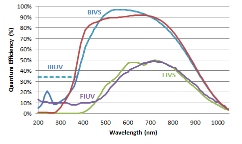
Quantum Efficiency by type of CCD

*OE- open electrode, FIUV- front illuminated UV enhanced, FIVS- front illuminated visible, BIUV- back illuminated UV enhanced, BIVS- back illuminated visible, BIDD- back illuminated deep depletion
Selection of all HORIBA Spectroscopy CCD’s
|
Cooling |
Type* |
Peak QE |
Array Dimension |
Pixel Size |
|
|---|---|---|---|---|---|
|
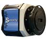
Syncerity |
TE -60°C |
OE |
58% |
1024 x 256 |
26µm x 26µm |
|
TE -50°C |
BI NIR |
84% |
2048 x 70 |
14µm x 14µm |
|
|
TE -50°C |
BI UV-VIS |
78% |
2048 x 70 |
14µm x 14µm |
|
|
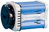
Synapse CCD |
TE -75°C |
OE |
58% |
1024 x 256 |
26µm x 26µm |
|
FIVS |
56% |
1024 x 256 |
26µm x 26µm |
||
|
FIUV |
58% |
1024 x 256 |
26µm x 26µm |
||
|
BIVS |
95% |
1024 x 256 |
26µm x 26µm |
||
|
BIUV |
75% |
1024 x 256 |
26µm x 26µm |
||
|
BIDD |
95% |
1024 x 256 |
26µm x 26µm |
||
|
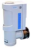
Symphony II CCD |
LN2-133°C |
OE |
58% |
1024 x 256 |
26µm x 26µm |
|
FIVS |
56% |
1024 x 256 |
26µm x 26µm |
||
|
FIUV |
58% |
1024 x 256 |
26µm x 26µm |
||
|
BIVS |
95% |
1024 x 256 |
26µm x 26µm |
||
|
BIUV |
75% |
1024 x 256 |
26µm x 26µm |
||
|
BIDD |
95% |
1024 x 256 |
26µm x 26µm |
*OE- open electrode, FIUV- front illuminated UV enhanced, FIVS- front illuminated visible, BIUV- back illuminated UV enhanced, BIVS- back illuminated visible, BIDD- back illuminated deep depletion
EMCCD
UV-VIS-NIR EMCCDs
Quantum Efficiency by type of EMCCD
*FIUV- front illuminated UV enhanced, FIVS- front illuminated visible, BIUV- back illuminated UV enhanced, BIVS- back illuminated visible, BIDD- back illuminated deep depletion
Selection of Synapse EMCCDs
|
Cooling |
Type* |
Peak QE |
Array Dimension |
Pixel Size |
|
|---|---|---|---|---|---|
|
Synapse EMCCD |
TE -60°C |
FIVS |
49% |
1600 x 200 |
16µm x 16µm |
|
FIUV |
49% |
1600 x 200 |
16µm x 16µm |
||
|
BIVS |
95% |
1600 x 200 |
16µm x 16µm |
||
|
BIUV |
95% |
1600 x 200 |
16µm x 16µm |
||
|
BIDD |
92% |
1600 x 200 |
16µm x 16µm |
*OE- open electrode, FIUV- front illuminated UV enhanced, FIVS- front illuminated visible, BIUV- back illuminated UV enhanced, BIVS- back illuminated visible, BIDD- back illuminated deep depletion
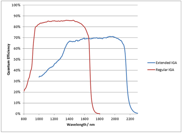
InGaAs Arrays
Near-IR InGaAs linear arrays
Quantum Efficiency by Type of InGaAs
|
Cooling |
Wavelength |
Array Dimension |
Element Size |
More Info |
|
|---|---|---|---|---|---|
|
Synapse InGaAs |
TE -60°C |
800-1650 nm |
512 x 1 |
25µm x 500µm |
|
|
1050-2100 nm |
512 x 1 |
25µm x 250µm |
|||
|
Symphony II InGaAs |
LN2-103°C |
800-1600 nm |
512 x 1 |
25µm x 500µm |
|
|
1000-2050 nm |
512 x 1 |
25µm x 250µm |
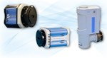
Nhà sản xuất: HORIBA Scientific
Các camera quang phổ được sử dụng kết hợp với các phổ và các phụ kiện liên quan đến phần mềm để xây dựng các giải pháp quang phổ tùy chỉnh.

Quang phổ Raman nhanh chóng trở thành phương pháp phổ biến để kiểm tra các cấu trúc và thành phần hóa học. HORIBA Scientific rất linh hoạt trong thiết kế hệ thống phát hiện phổ Raman dựa trên các linh kiện với sự lựa chọn các máy quang phổ iHR và CCD Synapse hoặc Symphony II và các detector InGaAs. Các hệ thống của chúng tôi phù hợp nhất với các nhà nghiên cứu muốn linh hoạt tối đa khi thu thập các dữ liệu quang học của riêng mình, kết nối với kính hiển vi có sẵn, hoặc đối với các nhà nghiên cứu có tài chính giới hạn mà cần hệ thống phát hiện độ nhạy cao có thể mở rộng và nâng cấp trong tương lai. Bộ phận Raman chuyên dụng của HORIBA Scientific cung cấp đầy đủ các hệ thống quang phổ Raman.

Các công nghệ quang phổ hấp thụ/truyền qua/phản xạ được sử dụng rộng rãi để xác định các tính chất của vật liệu. Tính module của hệ thống quang phổ HORIBA vượt trội hơn so với hệ thống quang phổ UV-VIS truyền thống bằng cách cho phép quý khách mở rộng các khả năng thí nghiệm. Cách tử kép tự động có thể hoán đổi kết hợp với bánh xe lọc phân loại trật tự được động cơ hóa, cổng ra kép của microHR và nhiều nguồn sáng và detector mang tới sự linh hoạt cần thiết cho toàn dải bước sóng từ 180nm đến 20micon.

Với các linh kiện quang phổ của HORIBA Scientific, khách hàng có thể thiết kế máy huỳnh quang tùy chỉnh bằng cách sử dụng các máy quang phổ iHR làm các máy quang phổ kích thích và phát xạ với sự lựa chọn các loại nguồn kích thích, buồng mẫu và detector. Điều khiển toàn bộ hệ thống bằng phần mềm Syner JY. Bộ phận Huỳnh quang HORIBA Scientific cung cấp rất nhiều máy quang phổ chuyên dụng và cả thiết bị huỳnh quang thời gian sống miền thời gian và miền tần số, là các thiết bị có độ nhạy cao nhất trên thị trường thiết bị phân tích và nghiên cứu.
 Schematic")
Phát quang là công nghệ đơn giản để phân tích vật liệu bán dẫn. Thiết bị iHR550 được trang bị detector CCD được làm mát trong dải 400-1000nm và một detector inGaAs trong dải 800-1600 là hệ thống đo phát quang tuyệt vời. Cấu hình quang học riêng có thể được thiết kế để PL trogn nhiệt độ phòng và nhiệt độ thấp sử dụng cùng máy quang phổ iHR. Các máy quang phổ iHR rất linh hoạt để thay đổi các thí nghiệm và cấu hình quang học để đáp ứng nhu cầu của khách hàng.

Việc ghi lại đồng thời các phổ tại nhiều điểm khác nhau trong plasma có thể cung cấp những thông tin quan trọng về các hiện tượng khác nhau trong không gian. Một sợi quang có nhiều đầu vào có thể thu ánh sáng từ nhiều điểm khác nhau trong plasma và sắp xếp các tín hiệu vào đường thẳng tại khe vào của phổ. Tận dụng độ phân giải cao của máy đơn sắc 1250M và độ nhạy cao của hệ thống CCD Symphony II làm mát bằng nitơ lỏng, các dữ liệu riêng biệt trong không gian thu được trên CCD và hiển thị các phổ phát xạ độc lập từ các điểm thu sợi quang khác nhau
Learn more about how multi-channel detectors are used in spectroscopy:
- CCD detectors in spectroscopy
- Wavelength to pixel correlation
- Image width and array detectors
- Multi-track spectroscopy
- Etalon fringing in back illuminated CCDs
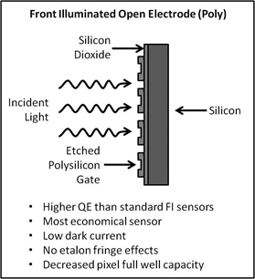
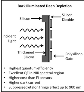
There are two main types of CCD sensors; front illuminated (FI) and back illuminated (BI). In a front illuminated sensor, the incident light must pass through the silicon gate before reaching the active silicon, generally leading to lower quantum efficiency. Response is typically low in the near-IR and UV, however lumogen coatings may be added to FI sensors to enhance UV response. To increase quantum efficiency in FI sensors, the polysilicon gate may be etched out to allow the light to pass more easily into the silicon layer. This type of sensor is often referred to as open electrode (OE) or open poly.
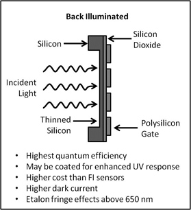
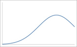
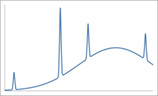
With a back illuminated sensor, the incident light strikes the photosensitive silicon layer directly. The silicon layer is physically thinned leading to higher quantum efficiency, but also causing etalon fringe effects from reflections between the silicon and silicon dioxide layers. Etaloning is a phenomena that can interfere with some spectroscopy measurements, but may have no interference for other measurements. For more information on etaloning, refer to our tutorial entitled “????”. To suppress etaloning and increase quantum efficiency, a thicker substrate may be applied to BI sensors. This type of sensor is referred to as back illuminated deep depletion. The graph below depicts the onset of etaloning in a standard back illuminated chip and a back illuminated deep depletion chip.

Schematics of each type of sensor are shown below with brief bullet points describing each sensor’s advantages and disadvantages.

When choosing a multi-channel detector, there are a number of parameters that must be considered. The first is wavelength range; different chip types have optimal efficiency in different spectral regions. For example, UV chips use a lumogen coating to enhance efficiency in the 200-400 nm spectral region, while back illuminated deep depletion chips have high efficiency in the NIR spectral region. In general, back illuminated chips will offer the highest quantum efficiency in any spectral range, however the type of signal being measured must also be considered.
Is the signal comprised of discrete spectral peaks like those seen in plasma measurements of atomic emission or is the signal broad and largely featureless as in many fluorescence measurements? The signal could also be a combination of both, for example in Raman measurements where discrete spectral peaks lie over a broad fluorescent background. For types of experiments that have broad signals or backgrounds in the VIS-NIR spectral region, front illuminated chips are a good choice as they do not suffer from etalon fringing evident in back illuminated chips.
Lastly, how intense is the light being measured? If the signal is very dim, integration times will necessarily be very long. In this case, a liquid nitrogen deep cooled camera is the best choice for highest sensitivity.
The table below provides a guideline for choosing the correct detector for your application organized by wavelength range and type of measured signal. There are other factors involved in choosing a CCD; HORIBA’s talented sales team can provide further guidance.
|
|
|
|
|
|
OE |
250 – 950 nm |
||
|
FIUV |
200 – 950 nm |
||
|
FIVS |
350 – 850 nm |
||
|
BIUV |
200 – 950 nm |
200 – 600 nm |
200 – 600 nm |
|
BIVS |
350 – 950 nm |
||
|
BIDD |
350 – 1050 nm |
||
|
InGaAs |
800 – 1700 nm |
||
|
Ext-InGaAs |
900 – 2200 nm |
||

*The wavelength ranges reported in this table indicate the optimal QE spectral ranges. For detailed spectral response, refer to the full quantum efficiency curves.
|
|
|
|
|
|
OE |
UV – VIS – NIR |
||
|
FIUV |
UV – VIS |
||
|
FIVS |
VIS |
||
|
BIUV |
UV – VIS |
UV – VIS (up to 600 nm) |
UV – VIS (up to 600 nm) |
|
BIVS |
VIS |
VIS (up to 600 nm) |
VIS (up to 600 nm) |
|
BIDD |
VIS – NIR |
VIS – NIR (up to 800 nm) |
VIS – NIR (up to 800 nm) |
|
InGaAs |
NIR (up to 1700 nm) |
||
|
Ext-InGaAs |
NIR (up to 2200 nm) |
||